Board-level wiring techniques
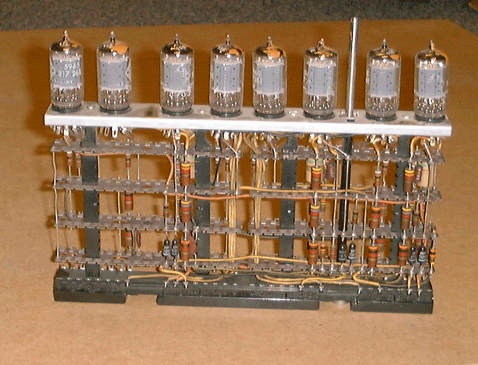
Detail of a wiring plane of the IBM 604 electronic calculator, ca. 1950. Tube assembly sockets are clearly visible. Because the tubes were mounted in assemblies (right picture) together with a number of components, the backplane wiring could be relatively simple.
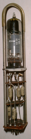
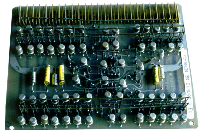
Module from an IBM 700 series computer, ca. 1957. The module has probably been built at IBM Sindelfingen (Germany), as it is equipped with Telefunken tubes.
Printed circuit board from a Bull/General Electric 235 computer, 1963. Notice the ground- and power rails. In a modern multi-layer circuit board, power is distributed through conductive planes embedded in the board.
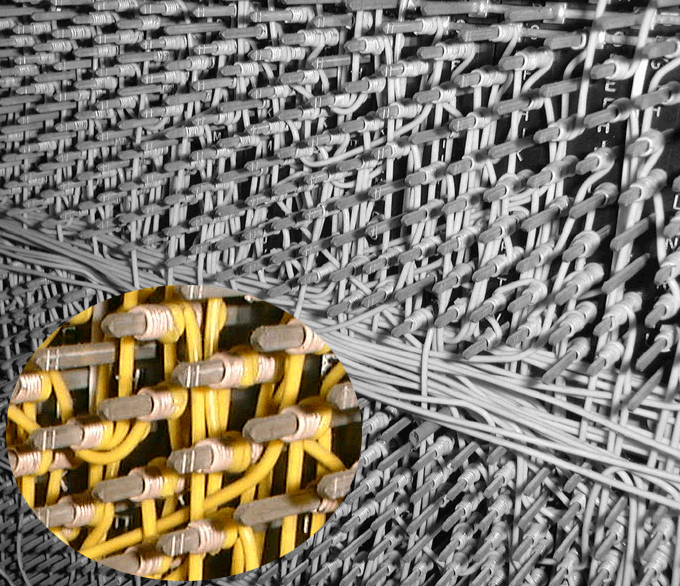
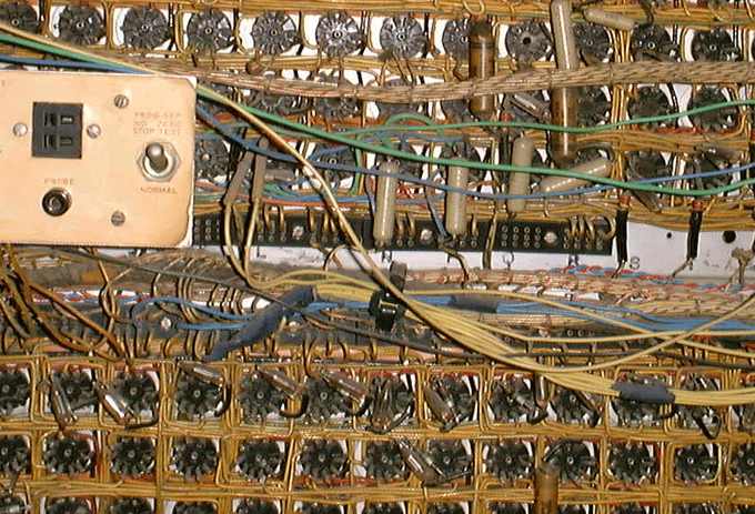
A wire-wrapped circuit board (backplane of the PDP-8 'classic').
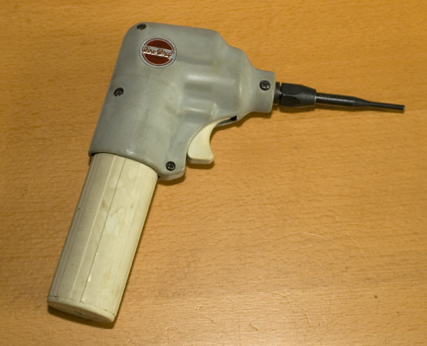
Wires are wrapped around protruding square gold- or nickel-plated
terminal posts using a
special tool, which automatically strips the Teflon insulation from the last few turns. (Winding a portion of
insulated wire around the terminal increases the connection's
ability to withstand stress and vibration). This procedure provides
very reliable connections and can easily be automatized.
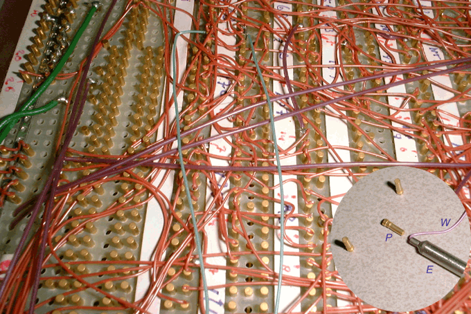
Wire bonding is used for experimental or semi-permanent set-ups. Wires W are welded
to the pins P by exerting force on the applicator tube E, put on
top of P with W in between. This locally removes the insulation
from W, and allows welding current to pass from E via the welding
spot and P to a counter electrode protruding from the surface the
breadboard is put on, component side down (but still without the
components). The pins P are hollow making it possible to insert IC
pins or component connection wires.
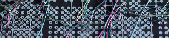
Below is a close-up example of wire bonding on an
Amdahl 580 chip carrier board (grid spacing 1 mm).